onsemi
NVMJS1D3N04CTWG
MFR #NVMJS1D3N04CTWG
FPN#NVMJS1D3N04CTWG-FL
MFRonsemi
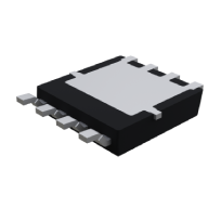
Part DescriptionMOSFET N-Channel 40V 41A (Ta), 235A (Tc) 3.8W (Ta), 128W (Tc) Surface Mount, 8-LFPAK
Datasheet
Quote Only
more info
Product Attributes
| Main Category | Semiconductors |
| Category | Discrete Semiconductors |
| Sub Category | Transistors |
| Family Name | NVMJS1D3N04C |
| Packaging Type | Tape and Reel |
| Packaging Quantity | 3000 |
| Lifecycle Status | Active |
| ROHS | Compliant with Exemption |
| RoHs Exemption Type | 7(a), RoHS (2015/863) |
| RoHs China | Not Compliant |
| Reach Status | Not Compliant |
| Package Type | 8-LFPAK |
| Channel Mode | Enhancement |
| Configuration | N-Channel |
| Drain Source Voltage | 40V |
| Drive Voltage | 10V |
| FET Feature | N/R |
| FET Options | N/R |
| FET Type | Single |
| Gate to Source Voltage | ±20V |
| Input Capacitance | 4300pF |
| Input Capacitance Test Voltage | 25V |
| Maximum Continuous Drain Current | 41A (Ta), 235A (Tc) |
| Maximum Drain to Source Resistance | 1.3 mOhm @ 50A, 10V |
| Maximum Gate to Source Threshold Voltage | 3.5V @ 170µA |
| Maximum Junction Temperature | 175°C (TJ) |
| Maximum Operating Temperature | N/A |
| Maximum Power Dissipation | 3.8W (Ta), 128W (Tc) |
| Maximum Pulse Drain Current | 900A |
| Maximum Total Gate Charge | 65nC |
| Maximum Total Gate Charge Test Voltage | 10V |
| Minimum Junction Temperature | -55°C (TJ) |
| Minimum Operating Temperature | N/A |
| Technology | MOSFET (Metal Oxide) |
| Typical Gate to Drain Charge | 12nC |
| Typical Gate to Source Charge | 20nC |
