onsemi
FQU13N06LTU-WS
MFR #FQU13N06LTU-WS
FPN#FQU13N06LTU-WS-FL
MFRonsemi
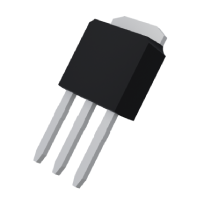
Part DescriptionN-Channel 60 V 11A (Tc) 2.5W (Ta), 28W (Tc) Through Hole I-PAK, TO-251AA
Datasheet
Quote Only
more info
Product Attributes
| Main Category | Semiconductors |
| Category | Discrete Semiconductors |
| Sub Category | Transistors |
| Family Name | FQU13N06L |
| Packaging Type | Tube |
| Packaging Quantity | 75 |
| Lifecycle Status | Obsolete |
| ROHS | Compliant with Exemption |
| RoHs Exemption Type | 7(a), RoHS (2015/863) |
| RoHs China | Not Compliant |
| Reach Status | Not Compliant |
| Package Type | I-Pak |
| Channel Mode | Enhancement |
| Configuration | N-Channel |
| Drain Source Voltage | 60V |
| Drive Voltage | 5V, 10V |
| FET Feature | N/R |
| FET Options | N/R |
| FET Type | Single |
| Gate to Source Voltage | ±20V |
| Input Capacitance | 350pF |
| Input Capacitance Test Voltage | 25V |
| Maximum Continuous Drain Current | 11A (Tc) |
| Maximum Drain to Source Resistance | 115 mOhm @ 5.5A, 10V |
| Maximum Gate to Source Threshold Voltage | 2.5V @ 250µA |
| Maximum Junction Temperature | 150°C (TJ) |
| Maximum Operating Temperature | N/A |
| Maximum Power Dissipation | 2.5W (Ta), 28W (Tc) |
| Maximum Pulse Drain Current | 44A |
| Maximum Total Gate Charge | 6.4nC |
| Maximum Total Gate Charge Test Voltage | 5V |
| Minimum Junction Temperature | -55°C (TJ) |
| Minimum Operating Temperature | N/A |
| Technology | MOSFET (Metal Oxide) |
| Typical Gate to Drain Charge | 2.7nC |
| Typical Gate to Source Charge | 1.6nC |
